- 您现在的位置:买卖IC网 > Sheet目录3818 > PIC18F4620-I/ML (Microchip Technology)IC MCU FLASH 32KX16 44QFN
PIC17C4X
DS30412C-page 180
1996 Microchip Technology Inc.
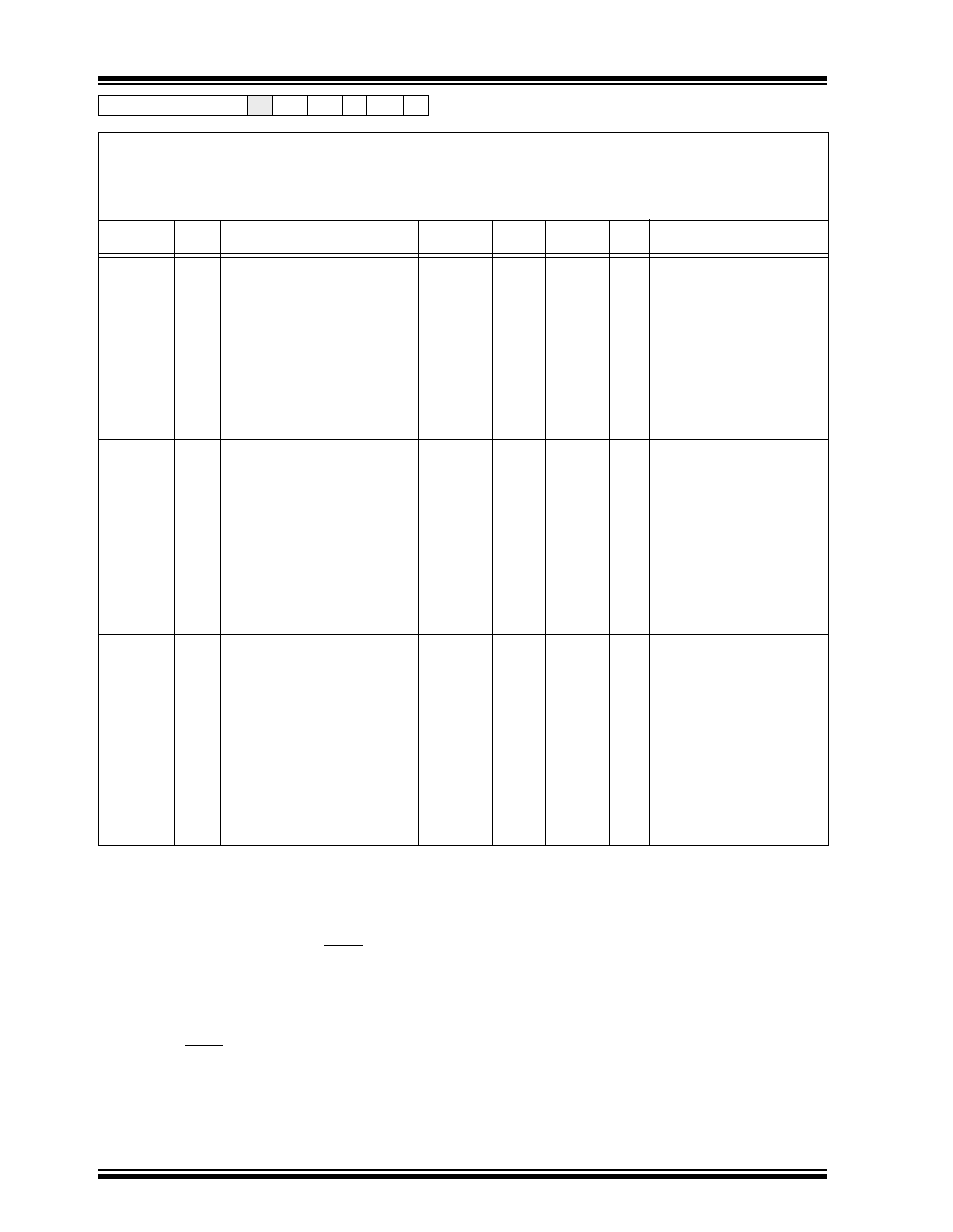
Applicable Devices 42 R42 42A 43 R43 44
Output Low Voltage
D080
D081
VOL
I/O ports (except RA2 and RA3)
with TTL buffer
–
0.1VDD
0.1VDD *
0.4
V
IOL = VDD/1.250 mA
4.5V
≤ VDD ≤ 6.0V
VDD
= 2.5V
IOL = 6 mA, VDD = 4.5V
Note 6
D082
RA2 and RA3
–
3.0
V
IOL = 60.0 mA, VDD = 6.0V
D083
D084
OSC2/CLKOUT
(RC and EC osc modes)
–
0.4
0.1VDD *
V
IOL = 1 mA, VDD = 4.5V
IOL = VDD/5 mA
(PIC17LC43/LC44 only)
Output High Voltage (Note 3)
D090
D091
VOH
I/O ports (except RA2 and RA3)
with TTL buffer
0.9VDD
0.9VDD *
2.4
–
V
IOH = -VDD/2.500 mA
4.5V
≤ VDD ≤ 6.0V
VDD
= 2.5V
IOH = -6.0 mA, VDD=4.5V
Note 6
D092
RA2 and RA3
–
12
V
Pulled-up to externally
applied voltage
D093
D094
OSC2/CLKOUT
(RC and EC osc modes)
2.4
0.9VDD *
–
V
IOH = -5 mA, VDD = 4.5V
IOH = -VDD/5 mA
(PIC17LC43/LC44 only)
Capacitive Loading Specs
on Output Pins
D100
COSC2 OSC2/CLKOUT pin
–
25
pF
In EC or RC osc modes
when OSC2 pin is outputting
CLKOUT.
external clock is used to
drive OSC1.
D101
CIO
All I/O pins and OSC2
(in RC mode)
–
50
pF
D102
CAD
System Interface Bus
(PORTC, PORTD and PORTE)
–
50
pF
In Microprocessor or
Extended Microcontroller
mode
DC CHARACTERISTICS
Standard Operating Conditions (unless otherwise stated)
Operating temperature
-40C
≤ TA ≤ +85C for industrial and
0C
≤ TA ≤ +70C for commercial
Operating voltage VDD range as described in Section 19.1
Parameter
No.
Sym
Characteristic
Min
Typ
Max
Units
Conditions
*
These parameters are characterized but not tested.
Data in “Typ” column is at 5V, 25
°C unless otherwise stated. These parameters are for design guidance only
and are not tested.
These parameters are for design guidance only and are not tested, nor characterized.
Note 1: In RC oscillator conguration, the OSC1/CLKIN pin is a Schmitt Trigger input. It is not recommended that the
PIC17CXX devices be driven with external clock in RC mode.
2: The leakage current on the MCLR pin is strongly dependent on the applied voltage level. The specied levels
represent normal operating conditions. Higher leakage current may be measured at different input voltages.
3: Negative current is dened as coming out of the pin.
4: These specications are for the programming of the on-chip program memory EPROM through the use of the
table write instructions. The complete programming specications can be found in: PIC17CXX Programming
Specications (Literature number DS30139).
5: The MCLR/VPP pin may be kept in this range at times other than programming, but is not recommended.
6: For TTL buffers, the better of the two specications may be used.
发布紧急采购,3分钟左右您将得到回复。
相关PDF资料
PIC24HJ256GP210-I/PT
IC PIC MCU FLASH 128KX16 100TQFP
PIC24HJ128GP310A-I/PF
IC PIC MCU FLASH 128KB 100-TQFP
DSPIC33FJ128GP310-I/PF
IC DSPIC MCU/DSP 128K 100TQFP
PIC16C66-20I/SO
IC MCU OTP 8KX14 PWM 28SOIC
DSPIC33FJ128MC510-I/PT
IC DSPIC MCU/DSP 128K 100TQFP
PIC16C66-20I/SP
IC MCU OTP 8KX14 PWM 28DIP
PIC18LF2620-I/SP
IC MCU FLASH 32KX16 28SDIP
PIC16F877-04I/P
IC MCU FLASH 8KX14 EE 40DIP
相关代理商/技术参数
PIC18F4620-I/P
功能描述:8位微控制器 -MCU 64KB 3968 RAM 36 I/O RoHS:否 制造商:Silicon Labs 核心:8051 处理器系列:C8051F39x 数据总线宽度:8 bit 最大时钟频率:50 MHz 程序存储器大小:16 KB 数据 RAM 大小:1 KB 片上 ADC:Yes 工作电源电压:1.8 V to 3.6 V 工作温度范围:- 40 C to + 105 C 封装 / 箱体:QFN-20 安装风格:SMD/SMT
PIC18F4620-I/P
制造商:Microchip Technology Inc 功能描述:IC 8BIT FLASH MCU 18F4620 DIP40
PIC18F4620-I/PT
功能描述:8位微控制器 -MCU 64KB 3968 RAM 36 I/O RoHS:否 制造商:Silicon Labs 核心:8051 处理器系列:C8051F39x 数据总线宽度:8 bit 最大时钟频率:50 MHz 程序存储器大小:16 KB 数据 RAM 大小:1 KB 片上 ADC:Yes 工作电源电压:1.8 V to 3.6 V 工作温度范围:- 40 C to + 105 C 封装 / 箱体:QFN-20 安装风格:SMD/SMT
PIC18F4620-I/PT
制造商:Microchip Technology Inc 功能描述:IC 8BIT FLASH MCU 18F4620 TQFP44
PIC18F4620T-I/ML
功能描述:8位微控制器 -MCU 64KB 3968 RAM 36 I/O RoHS:否 制造商:Silicon Labs 核心:8051 处理器系列:C8051F39x 数据总线宽度:8 bit 最大时钟频率:50 MHz 程序存储器大小:16 KB 数据 RAM 大小:1 KB 片上 ADC:Yes 工作电源电压:1.8 V to 3.6 V 工作温度范围:- 40 C to + 105 C 封装 / 箱体:QFN-20 安装风格:SMD/SMT
PIC18F4620T-I/PT
功能描述:8位微控制器 -MCU 64KB 3968 RAM 36 I/O RoHS:否 制造商:Silicon Labs 核心:8051 处理器系列:C8051F39x 数据总线宽度:8 bit 最大时钟频率:50 MHz 程序存储器大小:16 KB 数据 RAM 大小:1 KB 片上 ADC:Yes 工作电源电压:1.8 V to 3.6 V 工作温度范围:- 40 C to + 105 C 封装 / 箱体:QFN-20 安装风格:SMD/SMT
PIC18F4680-E/ML
功能描述:8位微控制器 -MCU 64KB 3328 RAM w/ECAN RoHS:否 制造商:Silicon Labs 核心:8051 处理器系列:C8051F39x 数据总线宽度:8 bit 最大时钟频率:50 MHz 程序存储器大小:16 KB 数据 RAM 大小:1 KB 片上 ADC:Yes 工作电源电压:1.8 V to 3.6 V 工作温度范围:- 40 C to + 105 C 封装 / 箱体:QFN-20 安装风格:SMD/SMT
PIC18F4680-E/P
功能描述:8位微控制器 -MCU 64KB 3328 RAM w/ECAN RoHS:否 制造商:Silicon Labs 核心:8051 处理器系列:C8051F39x 数据总线宽度:8 bit 最大时钟频率:50 MHz 程序存储器大小:16 KB 数据 RAM 大小:1 KB 片上 ADC:Yes 工作电源电压:1.8 V to 3.6 V 工作温度范围:- 40 C to + 105 C 封装 / 箱体:QFN-20 安装风格:SMD/SMT